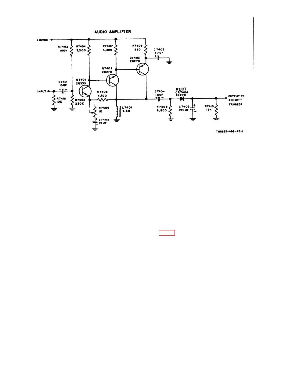
F i g u r e 1. Audio amplifier, schematic diagram.
(1) Transistor Q7602 receives its in-
secondary T7602, neutralizes the
put from the secondary winding of
second 11.5-mc amplifier. Capac-
T7602. The input signal is coupled
itor C7605 and inductor L7602 form
to the base of transistor Q7602
a decoupling network in the +16-
through capacitor C761O.
volt dc supply line.
(2) The output signal of Q7602 is de-
d. The output from the second 11.5-mc
veloped across a tuned circuit con-
amplifier is rectified by diode CR7602 and
sisting of inductor L7603 and ca-
filtered by capacitor C7613. The dc voltage
pacitor C7612. Resistor R7609
is taken from potentiometer R7611 and fed
reduces the Q of the tuned circuit
to the Schmitt trigger circuit. The amount
to provide the proper bandwidth.
of dc output voltage to the Schmitt trigger
(3) Resistors R7606 and R7607 form a
can be varied by adjustment of R7611.
voltage divider which provides the
fixed-biasing portion of the
5. Filter, 5.65-Mc
emitter-base bias for Q7602. Re-
sistors R7608 and R7605 establish
Filter FL7501 is a bandpass crystal
t h e self-biasing portion of the
filter having a center frequency of 5.65-
e m i t t e r - b a s e bias and stabilize
mc. The filter is in series with the output
t h e emitter current. Capacitor
of the test probe rf preamplifier circuit
C7609 is an rf bypass capacitor for
when switch S7902 is in position 12. It is
resistor R7605. Resistor R7608
a part of assembly A7500. The filter has a
pro vi d es emitter degeneration
minimum bandwidth of 5.4 kilocycles (kc)
which stabilizes the stage. The
at the 3-db points, a maximum bandwidth
stage is also stablized by the out-
of 6.6 kc at the 6-db points, and a maxi-
of-phase portion of the signal fed
mum bandwidth of 12.2 kc at the 50-db
to the emitter of Q7602 from the
points. Its input and output impedances are
tapped secondary winding of trans-.
50 ohms. Its insertion loss at 5.65 mc does
former T7602. Capacitor C7611, in
not exceed 6db
conjunction with the bottom half of
4


