
portion of the emitter-base bias
o f transformer T7702, trimmer
and stabilizes the emitter current.
capacitor C7708, and fixed capac-
Capacitor C7703 is an rf bypass
itor C7715. Resistor R7710 re-
duces the Q of the tuned circuit to
capacitor. Capacitor C7702 and in-
ductor L7701 form a decoupling
provide the proper bandwidth.
(2) Resistors R7709 and R7711 form a
network in the +16-volt dc supply
voltage divider which provides the
line.
f i x e d - b i a s i n g portion of the
c. The output from the 5.65-mc ampli-
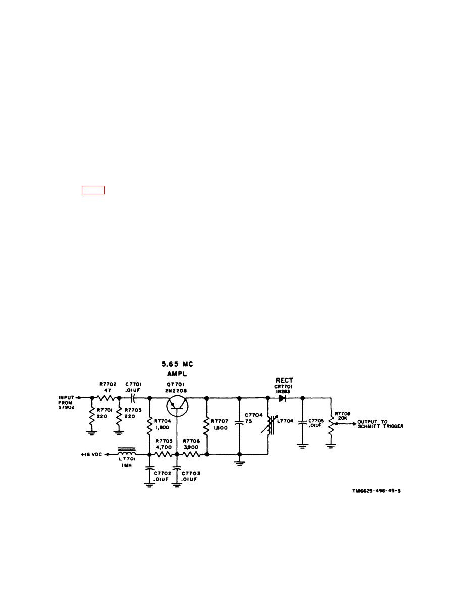
emitter-base bias for Q7702. Re-
fier is rectified by diode CR7701 and
sistors R7712 and R7713 establish
filtered by capacitor C7705. The dc output
t h e self-biasing portion of the
is taken from potentiometer R7708 and fed
emitter-base bias and are used for
to the Schmitt trigger circuit. The amount
c u r r e n t stabilization. Capacitor
of dc output voltage to the Schmitt trigger
C7707 is an rf bypass capacitor
can be varied by adjustment of R7708.
across R7713. Since only a portion
of the self-biasing network is rf
7. Amplifier, 47.0-Mc
bypassed, the input impedance of
Q7702 is effectively raised. Coil
The 47.0-mc amplifier is a two-stage rf
L7702 and capacitor C7710 form a
amplifier. Overall gain of the two stages is
decoupling network in the +16-volt
about 15 db. Power, input, and output con-
dc supply line.
nections to the 47.0-mc amplifier are made
b. The second 47.0-mc amplifier uses
when selector switch S7902 is in position
transistor Q7703 in a common-base stage.
18. The output from the 47.0-mc amplifier
(1) The `signal appearing at the sec-
is rectified and fed to the Schmitt trigger
ondary winding of T7702 is coupled
circuit.
through C7709 to the emitter of
a . The first 47.0-mc amplifier uses
Q7703. The output of Q7703 is
transistor Q7702 in a common-emitter
coupled through C7712 to the tuned
stage.
(1) The input signal from the test probe
output circuit which consists of
coil L7705 and capacitor C7713.
Resistor R7717 reduces the Q of
the tuned circuit to provide proper
(2) Resistors R7716 and R7715 form a
Figure 3. Amplifier, 5.65-mc, schematic diagram.
6
