TM 32-5811-025-14&P
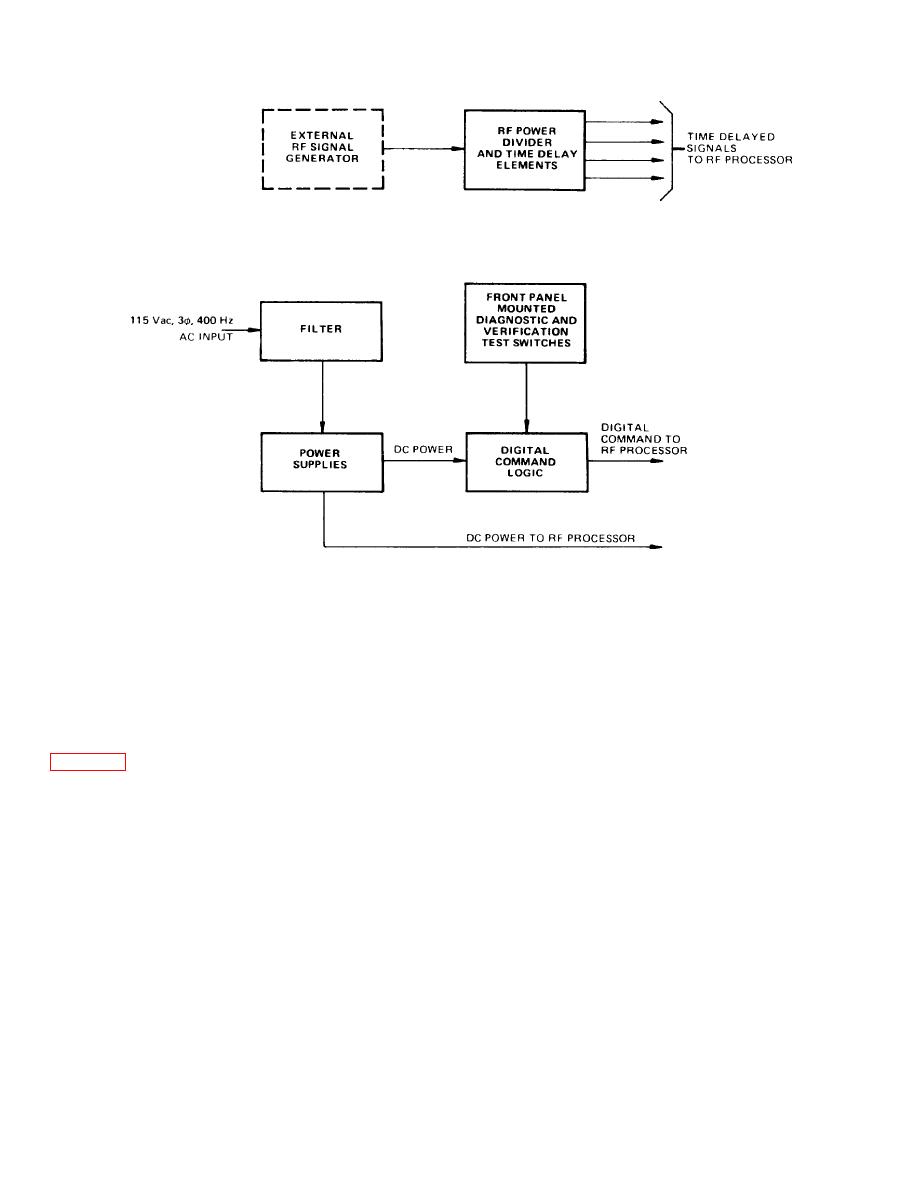
Figure 5-1. RF Processor Test Set Simplified Block Diagram
5-4. Parallel-to-Serial Converter CCA A1.
Parallel-to-serial converter CCA A1 contains a multiplexer that selects either the logic states set on
DIAGNOSTIC TEST switches S1 thru S17 and S19 or the logic states set in VERIFICATION TEST switch S18. During
the diagnostic test mode of the RF processor test set, the DIAGNOSTIC TEST switch inputs are selected for output from
the multiplexer. During the verification mode, the VERIFICATION TEST switch inputs are selected. The logic inputs
selected by the multiplexer are routed to a parallel-to-serial converter in the CCA. In turn, the CCA outputs a 24-bit serial
RF processor command word and associated clock to the RF processor under test. The output command word, shown in
figure 5-3, is used to set the switches and delay lines of the RF processor to the conditions chosen on the front-panel
DIAGNOSTIC TEST or VERIFICATION TEST switches.
5-5. RF Power Divider CP1.
RF power divider CP1 receives a signal from an external RF signal generator and provides four equal-amplitude
nondelayed outputs. Two of the outputs are routed to front-panel connectors J1 and J2 through transmission-line-type
time-delay elements. These elements
5-2


