TM 32-5811-025-14&P
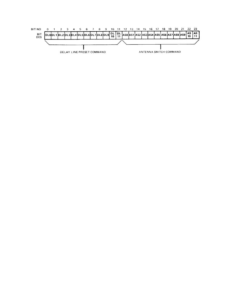
Figure 5-3. RF Processor Test Set Output Command Word
introduce 128 bits (12.8 ns) of delay into each line. The two remaining outputs of the power divider are routed directly
(without time-delay elements) to the RF processor under test through front-panel connectors J3 and J4. The RF
processor baseline select switches select specific time-delay offsets. The delay offsets are 000 bits, 128 bits, or 255 bits.
The RF processor test set does not provide a measurable offset of 255 bits. Rather, it supplies two pairs of in-
phase signals, where each signal in one pair is 128 bits out of phase when compared to each signal in the other pair.
The RF processor under test responds to test commands from the RF processor test set. It selects a pair of RF
processor power-divider outputs and sets its own internal delay lines. Each power-divider output selected is fed to one
RF processor internal processor delay line. The processes internal to the RF processor then result in offsets of 000 bits,
128 bits, or 255 bits of delay.
5-6. Power Supplies.
The power supplies contain electromagnetic interference (emi) filter FL1, which receives the RF processor test
set 115-V ac, 3- , 400-Hz primary input power. FL1 filters out unwanted electromagnetic interference from the input ac
primary-power lines. The filtered 115-V ac power is routed from the filter to the power supplies. When activated by the
front-panel-mounted POWER switch, the power supplies output regulated +5-V dc and 15-V dc supply voltages to the
RF processor under test. The +5-V dc power supply output also powers the various circuitry within the RF processor test
set. The 115 V ac, 3 , 400 Hz from emi filter FL1 is also used to power fan B1 in the RF processor test set. In addition,
the 115-V ac power is routed to the RF processor under test.
Section III. DETAILED THEORY OF OPERATION
5-7. General.
This section provides detailed circuit theory for the RF processor test set.
5-4


